PCB DESIGN BASICS: TURNING AN ELECTRONIC CIRCUIT INTO A RELIABLE PRODUCT

 EmTantra Technologies
·
·5 min read
·43 views
PCB DESIGN BASICS: TURNING AN ELECTRONIC CIRCUIT INTO A RELIABLE PRODUCT
A circuit may work perfectly on a breadboard, but that does not automatically mean it is ready to become a reliable electronic product.
When an electronic design moves toward production, the circuit must be converted into a printed circuit board (PCB) that is electrically reliable, mechanically suitable, manufacturable, and easy to test.
PCB design is therefore much more than connecting component pins with copper tracks. It is an important engineering stage that directly affects product performance, reliability, cost, and production quality.
At EmTantra Technologies, PCB development is part of our complete embedded product engineering process—from circuit design and component selection to firmware integration, testing, and product realization.
WHAT IS A PCB?
A printed circuit board is the physical platform that connects and supports electronic components.
A PCB typically contains copper traces, component pads, vias, solder mask, and a silkscreen layer. Depending on the design, it may use one, two, or multiple copper layers.
The PCB provides electrical connections between components while maintaining the mechanical structure of the electronic assembly.
PCBs are used in almost every modern electronic product, including IoT devices, industrial controllers, smart home systems, power supplies, communication gateways, and measurement instruments.
BEGIN WITH THE CIRCUIT AND REQUIREMENTS
Before starting the PCB layout, the schematic and product requirements should be reviewed carefully.
Important questions include:
- What voltage and current levels will the board handle?
- Which signals are sensitive to noise?
- Are high-speed communication interfaces used?
- Are there switching circuits, relays, or motor-control outputs?
- What are the enclosure dimensions and connector positions?
- What operating temperature and environmental conditions are expected?
- How will the board be assembled, programmed, and tested?
These requirements influence component selection, PCB layer count, placement, routing, clearances, and manufacturing decisions.
COMPONENT PLACEMENT MATTERS
Component placement is one of the most important stages of PCB layout.
A good placement strategy groups components according to their function and signal flow.
For example:
- Place decoupling capacitors close to the relevant IC power pins.
- Keep sensitive analog circuits away from noisy switching sections.
- Position connectors according to the enclosure and installation requirements.
- Keep power components arranged to support short and suitable current paths.
- Provide enough space for assembly, inspection, and rework.
Poor placement can make routing difficult and may introduce noise, thermal, or mechanical problems that are expensive to correct later.
PCB ROUTING AND SIGNAL INTEGRITY
Routing connects components using copper tracks.
Track width should be selected according to current, copper thickness, temperature rise, and the applicable design requirements.
For sensitive signals, routing should also consider return-current paths, coupling, impedance, and noise.
High-speed interfaces and switching power circuits may require additional layout controls. These depend on the signal frequency, edge rate, circuit topology, and product requirements.
A PCB should not be routed only to achieve the shortest visible connection. The complete electrical behavior of the circuit must be considered.
GROUNDING AND POWER DISTRIBUTION
Grounding and power distribution are essential for reliable operation.
A well-planned ground structure provides appropriate return paths for current. Poor grounding can create unwanted voltage differences, noise, and interference between circuit sections.
Power traces and copper areas must also be designed to handle the expected current without excessive voltage drop or heating.
In mixed-signal designs, the relationship between analog, digital, and power circuits should be evaluated based on the actual circuit architecture rather than applying a single grounding rule to every design.
DESIGN FOR MANUFACTURING AND ASSEMBLY
A PCB should be designed not only to function electrically but also to be manufactured consistently.
Design-for-manufacturing and design-for-assembly considerations include:
- Suitable component footprints
- Correct pad dimensions and spacing
- Appropriate solder mask and silkscreen clearances
- Assembly access and component orientation
- Panelization requirements
- Component availability and lifecycle
- Manufacturing tolerances
- Inspection and rework access
Incorrect footprints or unsuitable layout clearances can cause assembly problems even when the schematic is correct.
A manufacturing review before fabrication helps reduce avoidable delays and redesign costs.
ADD TESTING AND DEBUGGING ACCESS
Testing should be considered during PCB design—not after the board is assembled.
Useful design features may include:
- Test points for important power rails
- Programming and debugging connectors
- Access to communication interfaces
- Measurement points for critical signals
- Status LEDs where appropriate
- Space for production test fixtures
These features can make prototype debugging and production testing faster and more repeatable.
PCB DESIGN REVIEW BEFORE FABRICATION
Before releasing a PCB for manufacturing, the design should undergo a structured review.
A typical checklist includes:
- Schematic and PCB consistency
- Electrical rule check (ERC)
- Design rule check (DRC)
- Footprint and pin mapping verification
- Track width and clearance review
- Power and grounding review
- Connector and mechanical fit review
- Gerber and drill file verification
- Bill of materials and assembly output review
Automated checks are valuable, but they do not replace engineering review. A design can pass DRC and still contain functional, thermal, or manufacturability problems.
FROM PCB PROTOTYPE TO PRODUCTION
The first PCB revision is an important learning stage.
After fabrication and assembly, the board should be inspected and tested against the design requirements. Findings from bring-up and validation may lead to component changes, layout improvements, or firmware updates.
A disciplined revision process helps ensure that engineering changes are documented and that the correct design files are used for manufacturing.
CONCLUSION
PCB design is a critical part of building reliable electronic products.
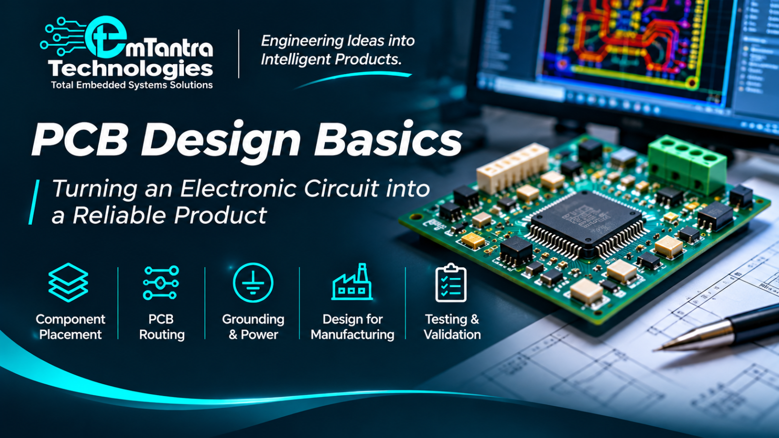
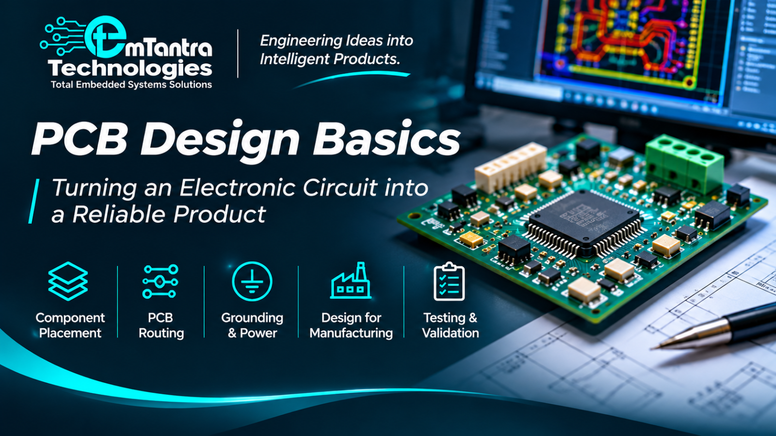
A successful PCB brings together circuit requirements, component placement, routing, grounding, manufacturing considerations, and testing access.
By considering these factors early, product developers can reduce redesign effort and improve the reliability and manufacturability of their electronic systems.
At EmTantra Technologies, we work on electronics design, PCB development, embedded firmware, IoT, and customized product engineering for industrial, agriculture, smart home, and connected-device applications.
Have an electronic product idea or need support with PCB development?
Visit emtantra.com to explore our engineering capabilities.
EmTantra Technologies
Total Embedded Systems Solutions
Engineering Ideas into Intelligent Products.